Capabilities
Etching
The Surface Technology Systems (STS) III-V Etcher, the Advanced Silicon Etcher, the STS Advanced Oxide Etcher (AOE), systems are all inductively coupled plasma (ICP) reactive ion etching (RIE) systems.
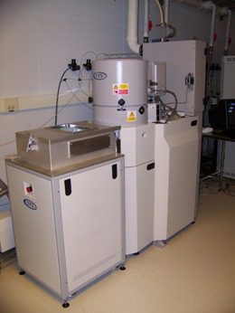
The STS systems provide a complete suite of etch capabilities, from high rate, high aspect ratio etching of silicon (STS ASE), high rate etching of dielectrics for microlens and waveguide applications, chlorine etching of III-V semiconductors, including GaAs, GaN, InP, GaP (STS III-V, Unaxis).
Deposition
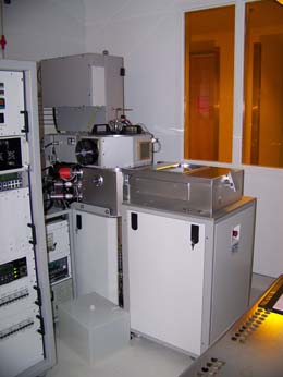
The STS Plasma Enhanced Chemical
Vapor Deposition System, used to deposit a wide range of inorganic and organic,
doped and undoped films, is capable of high deposition rates without compromising film properties and will accommodate substrates as large as 150 mm in diameter.
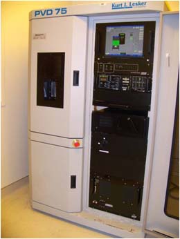
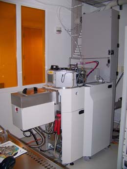
The tool provides thin film metal deposition by electron-beam and thermal evaporation techniques, and has the capacity to process three 100 mm wafers or a single 150, 200, or 300 mm wafer. For various types of thin film structures the AJA International ATC 1800-F Sputter Deposition system is in use as well.
Photolithography
The Quintel 4000 and 7000 series contact aligners use broad band UV to perform microscale lithographic exposures, including both front-side and back-side alignment capability. The systems accept substrates from 50 to 150mm, as well as pieces.
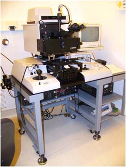
The GCA 5X Stepper, pictured (reduction step and repeat) projection system uses an exposure wavelength of 436 nm (g-line) lens column to provide a 5:1 reduction with a variable field size up to 15mm square. Wafer sizes of 3″ up to 150mm, as well as smaller pieces, can be accepted.
Nano-imprint Lithography
Molecular Imprints’ Imprio 100™ is a nanoreplication tool based on Step and Flash Imprint Lithography delivers high-resolution, sub-micron alignment, and 3-dimensional replication to sub-50nm lithography. Only the template fabrication process, typically with an e-beam writer, limits feature resolution.
Electron-beam Lithography
The Raith 150™
tool combines the ability to image nanoscale devices and structures with magnification factors of up to 1,000,000x with the ability to lithographically pattern substrates on a scale of 10’s of nanometers across a 150 mm pattern area.
Optoelectronic Fabrication and Packaging
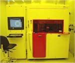
Various types of the COS (“chip-on-submount”) optoelectronic components can be fabricated for prototyping purpose by the following tools: Microautomation Dicing Saw, Loomis LSD-100 Scriber & Breaker (pictured), Finetech Lambda Flip-Chip Die Bonder , K&S 4524AD Wire Bonder.
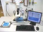
Optical and microwave test and
measurement facilities
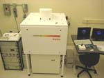
Fiber, waveguides, BER, EXFO OTDR (pictured).
Characterization and imaging
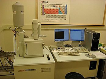
Interferometry, AFM, JEOL SEM (pictured), ellipsometry, Circular dicroism.
Numerical modeling

COMSOL, RSoft, CST Microwave Suite, custom MatLab simulations.